
2024.1.23:Clarity in Complexity: Meeting Electromagnetic Design Challenges for Electronic Systems (Commentary)
Key Takeaways
- Increase in cyber-physical systems design complexity: The information revolution has led to multifunctional PCB assemblies with smaller footprints, escalating circuit, package, and system design complexity. Increasing IC speeds, data rates, and denser configurations compound power integrity (PI), signal integrity (SI), and electromagnetic related (EMI/EMC) issues.
- Multiphysics Simulation Challenges: Electromagnetic (EM) simulations, crucial for tackling design challenges, are resource-intensive and are often segmented into smaller portions of the overall design to perform analyses, adding risk to design cycles. The addition of connectors further compounds EM high-frequency effects, necessitating careful analysis. As such, traditionally, EM analysis is done during the final verification step, leading to costly respins and/or redesigns when discrepancies are discovered late in the design cycle.
- EDA Workflow Inefficiencies: Conventional workflows require interfacing across multiple software tools for performing design and simulations, each with different user interfaces and product design databases, increasing the risk of design errors. Traceability of design changes and product configuration management are also a major challenge with disconnected tools and processes.
- Wireless and Heterogeneous Connectivity Demand: Technology proliferation drives a need for wireless connectivity across devices with various communication protocols, necessitating robust EM simulation to prevent interference.
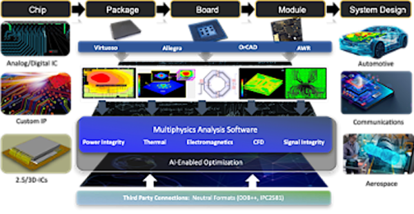
- The Cadence® electronic design automation (EDA) software suite for IC, advanced packaging, and PCB design, leveraging the Clarity™ 3D Solver for early-stage design and analysis of critical electronic assemblies and interconnects, facilitates designers to tackle EM and related multiphysics design challenges in complex electronics systems used in 5G/6G, aerospace and defense, automotive, and high-performance computing (HPC) applications.
Role of Multiphysics Analysis in Electronics System Design
Multiphysics analysis in electronics system design provides a holistic understanding by simulating the complex interactions among electrical, mechanical, thermal, and fluid dynamics phenomena within a system. This analysis is pivotal for optimizing performance as it enables designers to minimize thermal stress, reduce power consumption, and improve signal integrity by understanding the interplay of various physical phenomena. By simulating realistic operating conditions early in the design process, multiphysics analysis helps identify potential issues, thereby reducing development time and costs as problems can be rectified before physical prototyping. Design analysis and optimization significantly enhances system reliability and longevity by ensuring they operate well under a wide range of conditions and can withstand physical stresses over time. It provides a solid, data-driven foundation for making informed decisions regarding material selection, geometric design, and operational parameters, which are crucial for the efficiency and effectiveness of the system. Furthermore, multiphysics analysis ensures regulatory compliance and safety by helping designers adhere to standards concerning EMI/EMC, and thermal management. It fosters innovation by allowing the exploration of new design concepts, materials, and architectures in a virtual setting, which is conducive to the development of novel solutions. Employing multiphysics analysis can lead to product differentiation by enabling the creation of novel, high-performance, and reliable electronic systems. Tools like the Cadence Clarity 3D Solver are part of the broader multiphysics analysis ecosystem, aiding in electromagnetic simulation, which is crucial for tackling complex challenges in electronic system design. Overall, multiphysics analysis is indispensable in modern electronic system design, enabling designers to navigate the complex challenges inherent in the interplay of various physical phenomena, and ensuring the development of robust, efficient, and compliant electronic systems.[1]
Electromagnetic Challenges in Electronics System Design
Today’s high-performance electronic systems are being driven by ever-increasing complexity and IC density, requiring designers to consider EMI and EMC, as well as PI/SI and high-speed RF/microwave issues. To accelerate the design process and meet aggressive delivery schedules, engineers need to be able to perform EM cross-fabric and multiphysics analysis to model, simulate, and analyze these effects on chip, package, PCB, and system-level design. As such, there is a significant shift in electronics product development, where multiphysics EM simulation and analysis are being integrated earlier in the design process, unlike the traditional approach of evaluating them later in the detailed design and prototyping process. This shift mirrors trends seen in automotive and aerospace sectors such as simulation-driven design, aiming to identify and rectify design issues earlier, thus saving time and resources and improving “first build” quality. The acceleration of this “shift left” methodology in electronic system design is further propelled by enabling new AI and data-driven techniques. The rapid adoption of this approach in electronics system design is crucial for staying competitive in this fast-paced market.
In applications like 5G/6G, aerospace and defense, automotive, and high-performance computing (HPC) applications, the data speeds and volume are escalating at an exponential rate. Conducting crosstalk analysis and simulation in high-speed design becomes a Herculean task without the right field solver tools or analytical models. Modern high-speed PCB designers need to meticulously consider single-ended and differential crosstalk, along with power integrity problems that can be mistaken for crosstalk. A nuanced understanding of the relationship between physical design and overall system performance is crucial.
EM analysis is critical for uncovering any unintended EM interactions in the overall system and to ensure the design will meet performance specifications. In addition, EM simulation is used when designing a chip, package, board, or system to optimize the current design by looking at the results of the simulation and then fine tuning to further improve the key design parameters. Finally, EM simulation is important during the signoff phase when the design is complete, and it is necessary to confirm that it is fully optimized and meets specifications.
Clarity 3D Solver: Integration of Electromagnetic Design, Analysis, and Simulation
As noted, the EM simulations required to understand and address these design challenges traditionally have been analyzed by breaking up the system into multiple subsections and smaller parts, requiring large amounts of analysis time and computational resources. In addition, most workflows require multiple tools with different user interfaces, different file infrastructures, and design databases to accomplish various design and simulation tasks, while EM analysis and optimization are typically performed as a final step during design verification and signoff. All these issues can lead to costly errors that require design rework and delay time to market as defects in product performance vs. design requirements are uncovered late in the product development process, often during hardware build. The Cadence Clarity 3D Solver EM simulation software tool enables designers of PCBs, IC packages, and systems to overcome the most complex EM challenges in systems 5G/6G, aerospace and defense, automotive, and high-performance computing (HPC) applications (Figure 2).

(Courtesy Cadence)
The Clarity 3D Solver is a helpful tool for designing important connections in different types of electronic designs, and it’s built to tackle complex electromagnetic challenges quickly and accurately. Its special technology uses multiple computer cores and cloud resources to handle large, complex structures efficiently. This solver works smoothly with other Cadence design tools, creating a unified platform for high-speed and high-frequency design tasks. As fast connectors become more common, the Clarity 3D Solver helps in optimizing the connections between these connectors and other electronic components, meeting the needs for speed, capacity, and efficient memory usage. Additionally, its connection with the AWR Design Environment® platform helps in handling large electromagnetic problems without breaking them down into smaller parts, making design optimization and checking faster. The Cadence Optimality™ Intelligent System Explorer, which is integrated with Clarity is a new optimization platform aided by AI technology. The use of AI technology along with the Clarity 3D Solver is a step towards the future, pushing the electronics industry towards a scenario where design improvement is a continuous process aiming for better results.

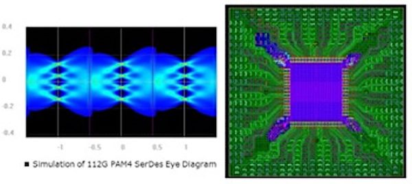
Case Study: Global Unichip Corporation (GUC) Achieves 5X Speedup of System Analysis for 112G Long-Reach Network Switch
GUC effectively integrated the Clarity 3D Solver in designing a complex network switch, achieving a 5-times boost in simulation performance and enabling pre-tapeout analysis to optimize the design for maximum performance at a lower cost. Additionally, by utilizing an integrated Cadence IC packaging design and analysis solution, including the Clarity 3D Solver for interconnect modeling and Sigrity™ SystemSI™ technology for evaluating 112G signal quality, GUC streamlined its design process, developing an efficient and holistic design methodology.
“As an ASIC design leader, delivering advanced designs to our customers in a timely manner is critical,” said Mr. Igor Elkanovich, CTO of GUC. “Enhanced performance for 3D finite-element method interconnect modeling was a key requirement for a successful collaboration. The Clarity 3D Solver delivered high-performance computational 3D full-wave modeling with gold-standard accuracy, enabling us to achieve optimized signal and power integrity along with a faster path to design closure. With a complete Cadence flow for design, analysis, and signoff, we completed the design of a complex networking application for our customer.”
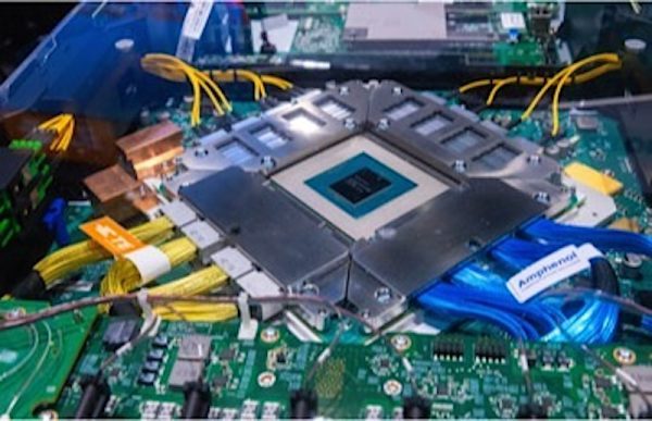
Case Study: Wistron Deploys Cadence AI-Driven Multiphysics System Analysis Solution to Dramatically Accelerate Product Development
Wistron, a leading technical service provider (TSP) adopted and deployed Cadence’s new AI-driven EM in-design analysis workflow, including the Optimality Intelligent System Explorer and the Clarity 3D Solver, to design a complex 800G network switch. Using the Optimality Explorer’s AI-driven optimization technology and the Clarity 3D Solver for fast, accurate, and scalable EM in-design analysis, Wistron was able to analyze large volumes of data―improving overall design reliability while realizing a significant reduction in turnaround time.
“By adopting Cadence’s AI-driven optimization solution including Optimality Explorer alongside the Clarity 3D Solver for our 800G network switch and GPU server, we leveraged the design of experiments model to explore multiple simulations quickly and realized far more robust designs,” said Mr. Christopher Huang, vice president of the Enterprise and Networking Business Group at Wistron. “With a shift left of AI-enabled multiphysics systems analysis into our electronic design workflow, we are not only improving product performance but gaining valuable design insight and engineering efficiencies.”
Concluding Remarks
The system design complexities inherent in today’s multifunction electronic products combined with increasing speeds and data transmission rates, decreases in power-supply voltages, and denser, smaller geometries produce many challenges for PI/SI, RF/microwave, and EMI/EMC designers.
The Clarity 3D Solver EM simulation software tool provides in-design EM simulations early in the process, delivering speed, accuracy, and scalability through a massively parallelized matrix solver. Because the Clarity 3D Solver is tightly integrated with Cadence’s other industry-leading multiphysics analysis tools, Cadence is now providing a complete model-based design and analysis workflow within a single commercial software platform. And the new Optimality Intelligent System Explorer now brings the power of AI to the EDA design process, which promises to make a significant impact on the ability to optimize electronics systems designs while also reducing the time to market and costs of complex electronics systems product development.
As such, CIMdata believes this integrated EDA design and analysis suite of tools can provide Cadence’s EDA customers with significant business benefits when utilized starting in the up-front conceptual design stage and carried forward throughout the detailed product design and development lifecycle.
[1] Research for this commentary was partially supported by Cadence.